As a leading company of image sensors, Sony Semiconductor Solutions has been responding to any demands with a wide-ranging product portfolio that includes products from compact to large sizes, from low speeds to high speeds, from low pixel counts to high pixel counts, and from ultraviolet light to infrared light. In addition, the package pin assignment has been standardized per series to make it easier to expand the deployment of the lineup in machine vision camera development. Image 1 shows the future evolution of the image sensors. Three axes have been defined as the directions of evolution. As representative examples of the performance improvement that forms the base of the first of these axes, this article introduces the simultaneous achievement of higher resolution and smaller sizes, and also technology for larger image sensor sizes and high speed readout. The second axis examined is the perspective of performance expansion from imaging to sensing. The new sensing technology introduced is SWIR image sensors. The third axis is functional expansion that is optimized as an edge system.
Higher Resolution & Smaller Size
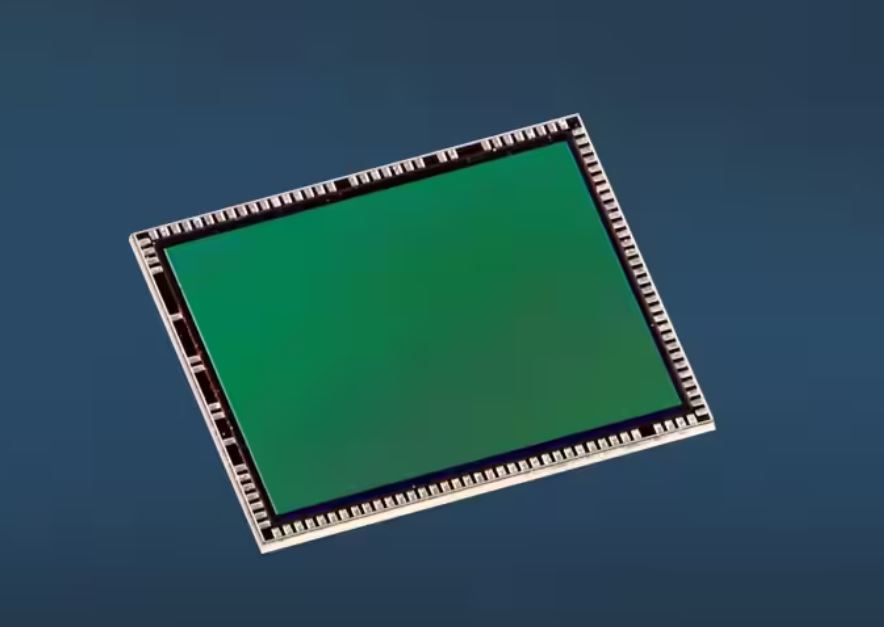
In visual inspection processes to detect items such as minute scratches and foreign particles, the demand for even higher inspection accuracy can be met by simply increasing the number of pixels in the image sensor. However, this creates the issue that it increases the chip size, which was previously a problem as it would also make the camera larger. Conversely, if the pixel size was reduced to maintain the camera size, the light collection area per pixel would be reduced, and the resulting deterioration in image quality made a reduction in recognition and inspection performance unavoidable. To address these issues, Sony developed the technology for a stacked CMOS image sensor which is equipped with a global shutter function and uses a back-illuminated pixel structure (Pregius S). This sensor is suitable for the industrial sector and simultaneously achieves both higher resolution and a smaller size. This new structure has a superior light collection efficiency compared to the conventional front-illuminated structure. In addition, the development of technology to block the light entering the memory area adjacent to the pixel has enabled the miniaturization of the pixel area to 2.74µm square, which is about 63% of the conventional models. Furthermore, the stacked integration of the signal processing circuits that were previously arranged around the pixel has simultaneously achieved both 1.7 times higher definition (12.37MP to 20.35MP) and a reduced package size (91% of the conventional model*1) with the same optical system.


