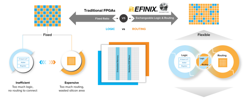
In a typical application the camera module will deliver a HDMI signal that needs to be converted to SDI with a small electronic assembly normally done in the camera’s housing. This requires the assembly to fulfill requirements in both low power dissipation for not distributing to heating the camera sensor and a small size to fit in the same housing. On the receiving side the SDI needs to be converted again either back to e.g. HDMI or directly fed into a frame-grabber. Efinix FPGAs combine low power consumption with high performance, making them an excellent fit for this type of application. This advantage comes from the company´s patented logic cell innovation, the FPGA’s smallest building block, the XLR cell. By integrating both logic and routing capabilities within the same cell, this architecture delivers more speed and efficiency while maintaining low power.
Driving 4K@60Hz video requires handling a pixel clock of around 600MHz, which the FPGA must process efficiently. In the specific use case discussed, the FPGA also needs to receive HDMI 2.0 with three data lanes at 6Gbps. After receiving, decoding, reformatting and potentially doing image processing, the video then needs to be converted into SDI format and transmitted via 12Gbps to a SDI cable driver. On the receiving end, the inverse is done. Again the Efinix SerDes in combination with the logic offers low power dissipation compared to other comparable devices.
Implementation on the Camera
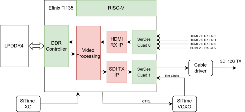
In the following the overall design idea of such a system is presented and key components are highlighted. Figure 2 shows the block diagram of the implementation located on the camera. The key components are the Ti135 with two SerDes Quads. The reference clock for the SerDes, the oscillator for the FPGA logic, the LPDDR4 external memory and the SDI cable driver. All blocks in green are hardened IP in the Efinix FPGA whereas the red blocks are soft IP by eVision-Systems. These System Verilog soft IPs have been developed in close cooperation with Efinix FAEs to ensure optimal integration with the transceiver and LPDDR4 hardened IPs. The hardened IP blocks (shown in green) offer the advantage of not consuming any FPGA fabric resources and are always more power-efficient than soft IP implementations. The functionality is as follows: Quad 0 is used for receiving the HDMI signal. As the HDMI signal can basically have any pixel clock, the HDMI clock signal needs to be used as reference clock for the Quad. Quad 1 is then used for transmitting a up to 12G SDI signal. All other lower SDI rates are supported as well. Depending on the application the LPDDR4 can be used to implement frame rate conversion, downscaling or even complex image processing. Instead of HDMI-Input the Efinix FPGA can also directly interact with up to 2.5G CSI2 image sensors.
Clocking up to 70m
For the long reach SDI transmit path the right clocking is key. As SDI specifies up to 70m of coax cable at 12G the Inter-Symbol-Interference build up leads to a very degraded signal at the receiver. For best operation, the transmitter needs to use a ultra precise reference clock with lowest jitter possible. Because SDI is a synchronous video interface, there is a direct dependence of pixel clock to SDI Link-Rate. In case of no frame rate conversion, the pixel clock directly depends on the HDMI input. This leads to a need to regulate the reference clock for SDI according to the HDMI video input. This clocking challenge is solved with the SiTime VCXO SiT3372AI which gives a frequency stability of ±25ppm and simultaneously an optimal pull-range (±200ppm) for video clock regulation purposes together with an ultra-low 0.225ps RMS phase jitter. The SiTime device also includes the SiTime’s unique DualMems temperature sensing and TurboCompensation technology that compensates for any thermal gradients shock and vibration, making it very suitable for applications in harsh environments. This VCXO is also available in very small packages down to 3.2×2.5mm. The FPGA’s transceivers can be accessed and re-configured via APB (Advanced Peripheral Bus) to support dynamic link rate changes during runtime. This makes it possible to have a single bitstream that supports various video standards at once.
Complete Video Transmission Solutions
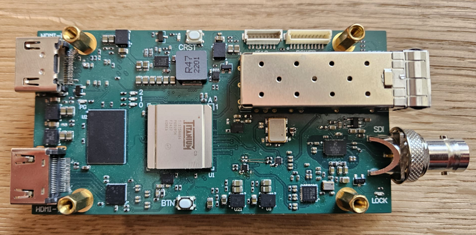
As an internal development platform, eVision Systems developed a PCB that integrates all necessary components to quickly prototype various applications with SDI and HDMI, as well as optical 10G Ethernet or optical SDI via an SFP+ cage. This new Efinix-based video technology architecture from eVision targets camera interface and video converter applications, enabling complete video transmission solutions for a wide range of markets, including medical, broadcast, and critical infrastructure. eVision Systems‘ video products are offered under the Aivion brand name.