Miniaturization is driving the development of micro-LEDs, also known as µLED. Micro-LEDs are miniature LEDs as small as a few microns. They are used as subpixels in next-generation miniature displays. In display technology, one image pixel consists of three to four subpixels that emit red, green or blue (RGB) light, and their combined output de-fines the color and brightness of the image pixel. Micro-LEDs of each primary color are grown on a semiconductor wafer in a high-precision manufacturing process similar to that of the semiconductor industry. They are then assembled to an array on a display panel that includes microelectronics to feed each pixel with an electric signal.
Unlike backlit display (i.e. LCD displays) every single LED pixel of a micro-LED display is an individual light source. Therefore, producing micro-LEDs and building micro-LED display panels is a challenging endeavor as the qual-ity of all micro-LED subpixels must be as consistent as possible. Today, it is technically impossible to ensure a 100 percent uniform performance of mass-produced micro-LEDs. The non-uniformity in luminance and colorimetry is clearly visible to the human eye, resulting in a non-acceptable image quality known as the mura effect.
Non-uniformity correction at subpixel level
The solution to compensate for this non-uniformity is a process called ‚demura‘. It consists of adjusting the input signal of each individual pixel so that the overall output of the array is uniform and patterns or artifacts are no longer perceivable to the human eye. However, display manufacturers can only apply this correction if they have accurate measurements of the luminance and colorimetry of every single micro-LED, along with their precise coordinates, so they can calculate the necessary correction and apply it to the right pixel. This requires very high-resolution apparatus with more than 100MP resolution and high-precision optics to deliver an accurate map with measurement values of every micro-LED along with their precise coordinates.
On-wafer and on-panel inspection
To meet these technical challenges, world-leading manufacturers of high-precision spectrometers, imaging systems and software solutions for spectral light measurement are developing state-of-the-art inspection systems that combine precision and speed. Fast inspection is critical to maximize production throughput and cut costs in an industrial environment. The system measures a series of parameters for every single micro-LED: pixel size and pixel pitch, dead or defective pixels, brightness/luminance, spectral/colorimet-ric characteristics, gamma/dynamic range, viewing angle, power/thermal behavior, and aging/burn-in. These measurements are performed either during LED-production on-wafer or after assembly as a display panel:
- On-wafer: Photoluminescence is used to quickly measure the performance of every single pixel in one image. A light stimulus in a specific wavelength is applied to the wafer, and the diodes react by emitting light in another wavelength, which is measured by the system.
- On-panel: The array is set to display a uniform color, and the system measures the luminance and colorimetry of every single subpixel.
Properly measuring the light beam of a micro-LED requires at least a four-time oversampling, meaning each micro-LED must be imaged by at least four pixels on the photometer’s image sensor. Being able to capture the full display in a single image is not only crucial for measurement tact time, it also improves mapping accuracy, as it eliminates the risk of errors in subpixel coordinates when shifting one image sensor to stitch several images of different display areas.
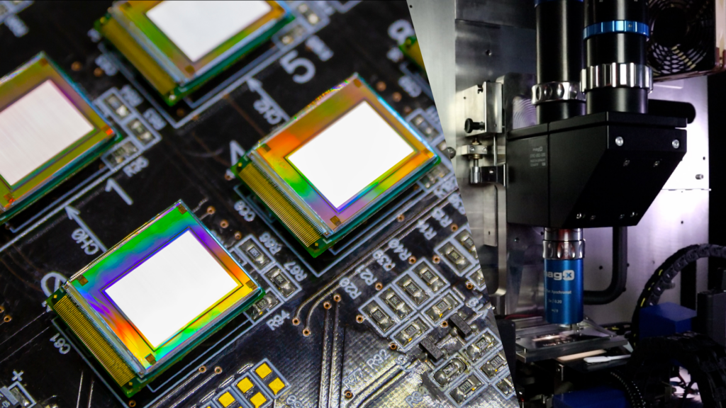
Microscopic system ensures high-precision
The high resolution of the image sensor can only unfold its full potential with the right optics. This is why micro LED inspection systems use the Excelitas Optem Mag.X 125 wide field industrial microscope. The microscope is essential to the overall system performance because it delivers high-resolution, large field of view (FoV), and consistently sharp image quality, even at the edges of the image. It supports large image sensor sizes up to 57mm. With its wide FoV, it allows the system to achieve micron resolution on a 5mm FoV. Optem Mag.X benefits from Excelitas‘ expertise in high-precision optics that nearly eliminates distortions and aberrations at the edges of the image, which is essential for the accuracy of the measurement of all micro-LEDs in the FoV. With further customization, the system can also integrate spectral filters needed for the photoluminescence inspection of micro-LED wafers.
In microscopic imaging, even minimal variations in the geometry of the object have an impact on the sharpness of an image. For example, if a wafer is not perfectly flat, some regions may become out of focus. The Mag.X series‘ built-in autofocus compensates for such variations and ensures crisp images at any time. Its high speed of operation ensures the imaging system can fulfill the demanding tact times of inspection in a manufacturing process.