Geometric deformation is particularly fatal to the disruption of the precision lithography process. Any significant warping (Warp) and bending (Bow) disrupts the focusing plane of the exposure system, leading to alignment failures and severe degradation of registration accuracy. At the same time, the inhomogeneity of the total thickness variation (TTV) directly affects the uniformity of film deposition and etching. According to the international semiconductor industry’s adopted standards such as ASTM F657, ASTM F534 and ASTM F1390, the calculation of several core parameters are crucial to the evaluation of wafer geometry.
Therefore, it is of importance to accurately measure and proactively control wafer TTV, Bow and Warp. TTV measures the uniformity of thickness across the entire wafer. It is calculated as the difference between the maximum thickness value and the minimum thickness value of all measurement points on the wafer surface. A large TTV means that the thickness of the wafer is uneven, which directly affects the flattening effect of chemical-mechanical polishing (CMP), the uniformity of thin film deposition, and may be out of the photolithography depth of focus (DoF) range. Bow describes the degree of concavity or convexity of the wafer’s center point relative to its edge reference plane in an unclamped free state. It primarily reflects the overall symmetrical curvature of the wafer as a bowl. According to ASTM F534, the reference plane is usually defined by three equidistant points on the edge of the wafer, and the Bow value is the distance from the center of the wafer to the plane defined by these three points. Warp is the most comprehensive measure of overall wafer flatness. It describes the total deviation of the highest and lowest of all points on the wafer surface relative to the Median Surface in the unclamped state. Unlike Bow, which focuses on the center point, Warp captures the full range of deformation incl. symmetric bending and all asymmetric distortions. A high Warp value usually means that significant residual stresses exist inside the wafer.
Confocal Chromatic Sensor Technology
The principle of confocal chromatic measurement is based on a specially designed objective lens with high Chromatic Aberration. When a complex-color light source (e.g., white light) passes through the objective lens, it undergoes spectral dispersion in the axial direction, forming a continuous array of focal points of different colors, each of which corresponds precisely to a unique spatial position. When light strikes the surface of the object under test, only the specific wavelength of light that happens to be focused on that surface is reflected back to the spectrometer with maximum intensity through the confocal pinhole. By decoding the peak wavelengths received by the spectrometer, the system can accurately invert the height (displacement) information of the measured point. Advantages of this technology include extremely high accuracy and resolution at the µm- to nm-level, non-contact measurement and powerful material adaptability
Measurement of wafer warpage
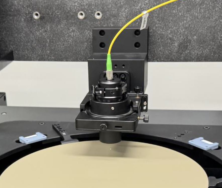
The wafer geometry parameter measurement equipment is usually configured for simultaneous measurement on both sides. The core structure is as follows:
- Dual probe system: On the upper and lower sides of the wafer transfer path, a confocal chromatic displacement sensor is installed respectively, and the optical axes of the two probes are aligned to achieve synchronized measurements on the upper and lower surfaces of the wafer. The distance (L) between the two probes is precision calibrated to a constant known value.
- High-precision scanning stage: The wafer is placed on a high-precision X-Y linear or rotating stage. During measurement, the platform drives the wafer in a high-speed, smooth movement, or the sensor itself moves on a gantry structure, thus rasterizing or helical scanning the entire wafer surface, collecting 3D coordinate data of millions of points to form a high-density point cloud map.
Through the above means, the spectral confocal measurement system not only provides three independent numerical results for TTV, Bow, and Warp, but also generates high-resolution 3D morphology and thickness distribution maps of the wafer. These visualization charts are invaluable for process engineers to analyze stress sources, optimize CMP or thinning processes, and diagnose equipment problems. Combining high accuracy, full size, non-destructive and high efficiency, confocal sensors have become a key technology support for incoming inspection, inline quality control (IPQC) and outgoing inspection (OQC) in semiconductor front-end and back-end processes.