The rapid advancement of semiconductor and integrated photonic system manufacturing has pushed surface tolerances into the sub-nanometer regime. For quality control and R&D, inspecting these delicate, transparent, or multi-layered materials is a persistent bottleneck. Traditional tools such as Atomic Force Microscopes (AFMs) offer sub-nanometer vertical resolution, but they are slow, requiring minutes or hours of mechanical raster scanning, and their physical probe tips risk damaging soft or delicate samples. Scanning electron microscopy (SEM) provides exceptional 2D lateral resolution but struggles with vertical height profiles and often requires destructive sample preparation, such as gold coat-ing inside vacuum chambers.
Standard optical phase profiling methods, such as Mach-Zehnder or Michelson interferometers, promise non-contact, high-speed measurements. However, these systems separate the light into distinct probes and reference optical arms. This separate-path architecture makes them extremely sensitive to environmental noise. In a manufacturing cleanroom or factory environment, this noise easily over-whelms the phase signal, requiring pneumatic vibration-isolation tables that prevent the systems from ever being integrated in-line on a fast-paced assembly line. Standard high-end optical microscopes are fast and non-destructive but they are blind to nanometer-scale vertical topography. For R&D teams, the penalty is time: slow, point-by-point characterization methods delaying time-to-market. Manufacturers face a costly choice: halt production for slow offline testing, or risk leaving critical defects undetected.
Common-Path Approach
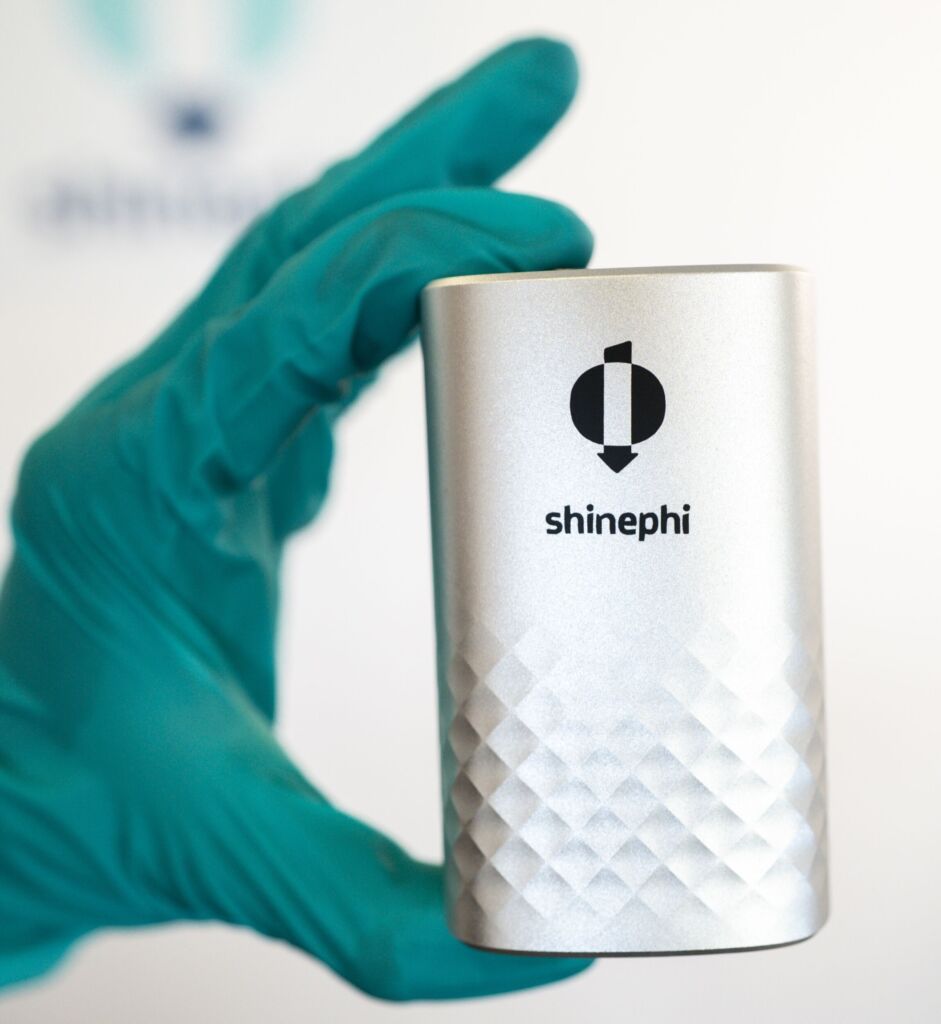
To bridge the gap between speed and sub-nanomet-ric precision, Shinephi has developed an innovative, patent-protected Lateral-Shearing Interferometric (LIM) technology designed as a compact, modular add-on phase camera (Fig. 1). In this configuration, the light is separated into a pair of orthogonally polarized beams which travel with a tiny, constant shear distance. Because the ‚original‘ and ‚copy‘ beams travel along nearly the exact same physical path, any environmental vibrations, temperature drifts, or air drafts affect both beams identically. Upon recombination, this common-mode noise cancels out completely. This common-path stability is what allows the imager to achieve a noise floor better than /1,000 in Optical Path Difference (OPD) without any active vibration isolation. In standard reflection mode this translates to an exceptional phys-ical vertical sensitivity of down to 0.1nm. Furthermore, the lateral resolution is determined directly by the optics used, easily resolving features down to ~1µm or smaller. The integrated module works in the visible spectrum (450-700nm) with standard illumination, for instance, a collimated LED light source in Köhler illumination mode.
By ‚plugging in‘ the module, an idle standard optical microscope can be converted into a high-speed, sub-nanometer metrology station, upgrading the engine of existing capital investments without the need for standalone, six-figure machines. The module can also be mounted to complementary systems like AFMs or spectroscopic setups to enable correlative metrology pipelines. This allows the user to survey wide-field topographies at video rates, pre-identifying areas of interest to guide localized point-by-point characterizations. By integrating the module inline directly into existing manufacturing or lithography setups, the system acts as an instant, real-time feedback loop. Instead of halting production to transport delicate substrates to slow, offline profiling stations, operators can catch nanometric process drifts immediately, preventing costly scrap events long before offline metrology would flag a defect.
Metrology Results
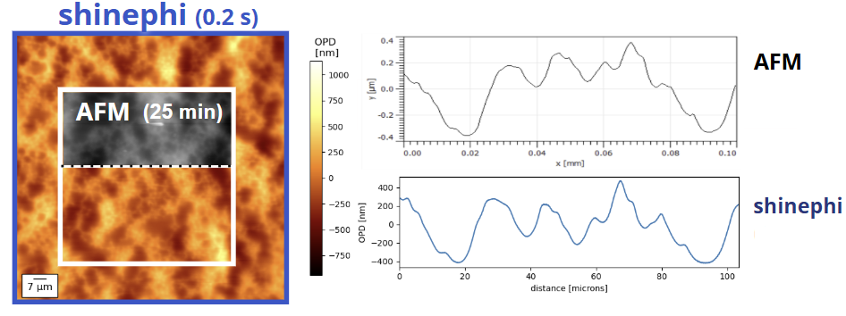
Under standard, un-isolated laboratory and factory-floor conditions, the LIM phase camera achieves a remarkable temporal noise floor better than /1,000 RMS in OPD. By capturing raw interferograms in a single shot at 50fps frame rate, the system enables ‚continuous scanning‘ pipelines where samples can be profiled on the move. To demonstrate the imager’s speed advantages, a structured glass surface was profiled in a direct comparison with a standard Atomic Force Microscope. While the AFM achieved superior detail, it required 25min of me-chanical raster-scanning to map a single region of interest. In contrast, the microscope-integrated phase module captured a larger field of view in 0.2sec. The 1D cross-sectional height profiles extracted from both instruments showed outstanding correlation, with profile variations attributable to sub-micron alignment offsets during sample positioning and different spatial resolution (Fig. 2).
www.shinephi.tech