Applications

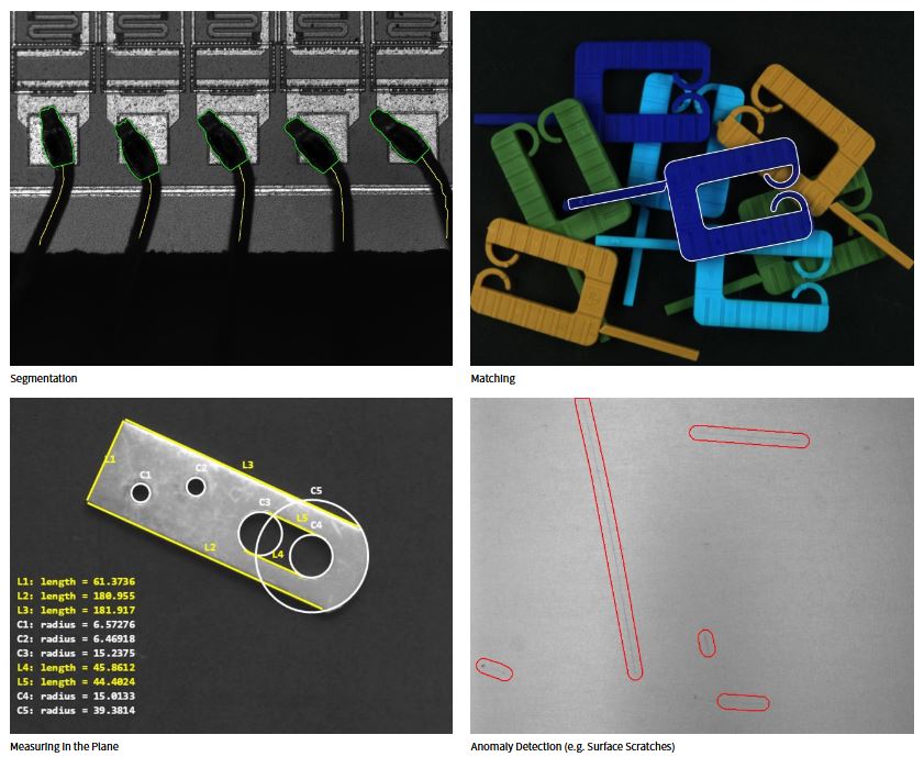
Silicon wafer inspection is an important application that can clearly leverage this new capability to see smaller features. The CQD cameras can be used to illuminate silicon wafers for: identifying front-to-back alignment marks, detecting voids in bonded wafers, imaging of for backside dicing, visualizing and detecting sub-surface cracks, and inspecting wafers for buried features, to name a few. Vision systems designed to inspect solar cells, glass bottles, and hosts of other industrial parts will now also see more. This higher resolving power can also be used to broaden the field-of-view, where machine vision cameras may now be configured to image both small and large format objects at the same imaging distance, with superior spatial resolution. Additional applications for the CQD cameras include: accurately identifying fill levels of transparent and opaque containers, inspection of embedded electronics, detection of moisture levels in packaged products, thickness and void detection on clear coat films, glass bottle imaging, bruise detection in fruits and vegetables, inspection of lumber products, detection of water/oil on metal parts, chemical analysis, imaging through smoke and mist environments, surveillance and security monitoring, crop monitoring, glucose monitoring and many more.


