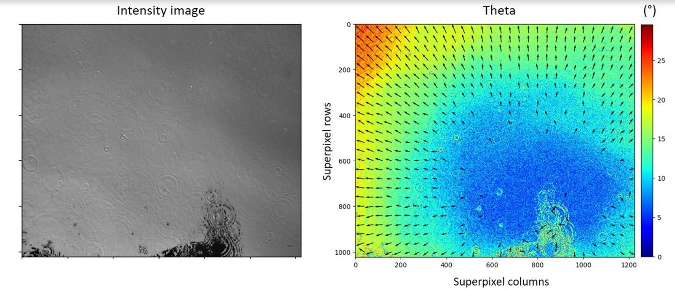
Dive-technology starts where the human eye and therefore also conventional image processing technologies (must) fail: Changes in properties often do not cause a clear change in colour, which can be tracked by capturing just three monochrome partial images (red, green, blue / RGB). This means that essential quality-determining sample parameters such as layer thickness, impurities, chemical composition, roughness, electrical conductivity, surface quality or the cleanliness of a surface remain optically invisible for conventional image-processing technologies. Further, Dive-technology enables several sample target parameters to be determined simultaneously, which conventional imaging inspection systems are usually incapable of out of physical reasons.
Hyperspectral Vision for Semiconductor Industry
Hyperspectral Vision technology, on the other hand, offers the simultaneous capture of several hundred monochromatic partial images, which is far superior to both the human eye and existing camera systems. The company´s technology makes it possible to comprehend the non-visible (hidden) properties of surfaces and thin layers quickly and non-destructively and to make them objectively usable for further work processes. The patented Hyperspectral Vision solution is comprehensive, contactless, and fast which makes it superior to existing inspection methods. In the past years over 60 development projects for industrial partners in various sectors show the potential for industrial use, including aerospace, automotive, glass manufacturing electrotechnology, and energy.
Applications in the semiconductor industry show an enormous potential with substantial customer commitment. The following issues, among others, have been successfully investigated in various projects in recent years:
- Spatially resolved layer thickness measurement of atomic layer deposition (ALD) layers on silicon wafers
- Spatially resolved detection and quantification of organic and/or anorganic impurities on wafers and films
- Quantification of organic impurities on copper surfaces for electronic components; production and sale of an inspection system for this application
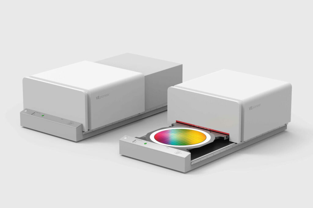
In November 2023 Dive has introduced the VEpioneer benchtop system solution for an easy use at-line in the production environment. Together with the VEsolve software inspection results can be achieved within 30 seconds by a 1-button-solution, whereby the user has access to an extensive pool of methods for data evaluation, which enables the simple use of machine learning and AI algorithms.
Location: Radeberg (Germany)
Year founded: 2023
Founder(s): Dr. Philipp Wollmann, Dr. Wulf Grählert,
Oliver Throl, Gösta Reißmann, Jan Güldemann
No. of employees: 9
Commercial status: revenue
Video: Company portrait